Bipolar Transistor (BJT) as a switch
When a transistor is used in a circuit, the behavior that it has will depend on its characteristic curves.
The diagram shows several curves representing the transfer function Ic (collector current) against VCE (collector voltage - Emitter) for various values \u200b\u200bof Ib (base current).
When the transistor is used as an amplifier, the operating point of it is located on a line of transfer functions that are in the active zone. (The lines are nearly horizontal).
Transistor in court and saturation
When a transistor is used as a switch or switch, the base current must have a value to make the transistor into court and another to enter into saturation
- A court transistor has a collector current (Ic) minimum (virtually zero) and a collector emitter voltage VCE) maximum (almost equal to the voltage supply). See the yellow area in Figure
- A transistor in saturation has a collector current (Ic) and maximum collector emitter voltage (VCE) close to zero (zero volts). See green area on the graph.
To make the transistor into court, the value of the base current should be low or even better, zero.
To make the transistor into saturation, the value of the base current should be calculated depending on the load being operated on and off (switch operation)
If you know which is the load current required to activate (it is a light bulb), it has the value of current that will drive the transistor when in saturation and the value of the power supply circuit, you can get the load line. See chart above.
This confirms that the load line for the transistor operating in saturation, Ic and VCE should be minimum and maximum to be in court, Ic should be the minimum and maximum VCE.
Design of a swich with Bipolar Transistor (BJT)
design example switch or switch to bipolar transistor
To calculate the value of Rb (base resistance) to be used for the circuit to operate as a switch (connect and ISCONNECT a voltage of 12 volts in A). See diagram.
The data we have are:
- Supply Voltage = 12 V
- Bulb (bulb) 12V, 1.2W
- B (beta) transistor is minimum: 200
Transistor in saturation
Ic For the following procedure:
From the formula of power: power = P = VXI bulb.
Solving I get: I = Ic = P / V = \u200b\u200b1.2 watts / 12 volts = 100 mA
We choose the B (beta) lower (200) to ensure that the transistor is saturated.
The base current is: Ib = Ic / B = 100 mA/200 = 0.5 mA.
This is the base current needed for the transistor Switch on and it becomes saturated cylinder.
To calculate whether Rb hare una mesh circuit based on it: 12 V x = Ib Rb - vbe
Rb = ( 12-0.7) / Ib = 3.11 V/0.5 mA = 2260 ohms. For practical purposes Rb = 2.2 kohms
Note: vbe = 0.7 volts in about a silicon transistor.
transistor cut
For the bulb goes off, enough that the current (Ic) that passes through it is zero. To achieve this means that the base current Ib is zero (Ic = BxIb), putting the voltage that feeds the core circuit to zero (0 volts)
Bipolar Transistor (BJT ) as iamplificador
is the most important practical application for the transistors used. The diagram shows a common-emitter amplifier stage:

The transistor has been polarized by polarization voltage division.
As we know, a high frequency capacitor behaves like a short circuit at low frequencies while it increases to behave like an open circuit for DC
Seen from this perspective should be analyzed in two-stage amplifier , one from the point of view of the CA and the other from the viewpoint of DC
This subdivision we analyze the circuit with two simpler circuits, which, thanks to the theory of superposition, what will happen is that the response will result from the sum total of the data obtained in the two circuits that broke the original.
begin the domain analysis of the CC, for this we take the following steps:
1 º) shorts out the generator is AC input.
2 º) capacitors are considered as open circuits.
3 º) the resulting circuit is analyzed. Opening
C1, C2 and C3 and shorting the generator input in our circuit we obtain the resulting circuit we see below:

Now, with the references already explained, we proceed to the resolution of the resulting circuit. With these data we obtain the bias point (Q).
CA For the analysis we turn to the following rules:
1 º) is short-circuited the power supply DC
2 º) capacitors are considered as closed circuit (short circuit).
3 º) is studied resulting circuit.
In the figure we see that as we proceeded to obtain the resulting circuit:

capacitors have disappeared from the circuit making shorts, the resistance disappears be R4 in parallel with a short circuit, the resistors R1 and R3 are now in parallel, so that we obtain Ra. Output resistors are the same thing happens, and we obtain Rb.
To complete our analysis we assume that we now apply a signal to the circuit and see how Q varies
point In the figure we see an example, which shows the point Q in the absence of signal and how it varies with the application of an input signal.
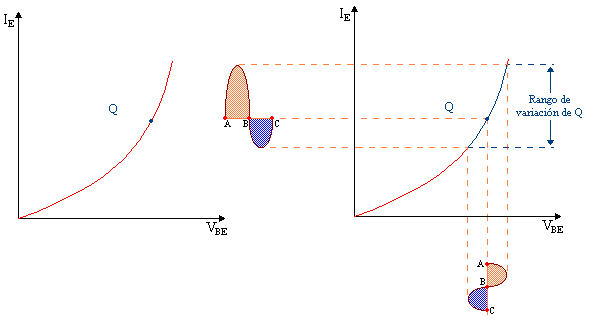
signal is seen that IE is not a direct correspondence applied to the base of the transistor since the curvature of the graph of the characteristic of the transistor.
is important to check carefully the place of location of the point Q, since if we want the transistor operates in the active region and polarize the latter at a point Q near the zone of saturation, we run the risk that when you apply an input signal, Q moves to the saturation zone, leaving the active zone. To avoid this problem should be analyzed variation ever before in our transistor Q and check that does not leave the region where we want to work.
Another important family of transistors is the field effect, which is part of the FET. They function as current control by a voltage applied to one of its terminals.
area are constructed with a P or N type semiconductor that links the two terminals (source and drain), this region is called the channel and on this there is another opposite sign that connects to the doorway between the two forms a pn junction or NP, depending on your topology. This set is mounted on a semiconductor with the same sign at the door. When voltage is applied between drain and source, current will flow through the channel.
this current control is done with a variable voltage is applied to the gate, and that by applying the voltage, the PN junctions are biased in reverse, causing the channel becomes thinner, and therefore, increase its resistance, thus creating a variation of the current flowing through it.
Door As this current is extremely weak because it is a reverse biased junction in, it will be possible to vary the current flowing through the transistor without the need to absorb power from it.
family also MOS transistors or MOSFET (Metal Oxide, Inc.) is part of the field effect transistors.
This type of transistor is made from a P-type semiconductor which broadcast two N-type regions forming the source and drain, and above the surface of these, apply a layer of silicon dioxide (SiO2), which has the property to be highly insulating, which is located on the door. Between source and drain will also exist similar to channel FET, whose strength and width will be controlled by the gate voltage.
The characteristic curves of the field effect transistors represents the drain current (ID) as a function of the applied voltage between drain and source (VDS). As in the case of transfer of bipolar transistors, draw a curve for each of the desired values \u200b\u200bof VGS. Also in these curves there are two areas, from the current source increases with stress, but reached a certain value Vp is constant and is formed from the second zone there, these two areas are called the linear region first and the saturation region last.
This type of transistors can be used in the circuits in an arrangement similar to that of the bipolar, ie common source, common drain and common gate, although the first and last are the most used in practice.
CRF
Z Lenny Perez M
0 comments:
Post a Comment