PN junction is called to the fundamental structure of electronic components commonly known as semiconductors, diodes and transistors mainly BJT. It consists of the metallurgical junction of two crystals, usually Silicon (Si), but also made of Germanium (Ge), P and N natures according to their composition at the atomic level. These glass types are obtained by doping pure metal crystals intentionally with impurities, usually metal or some other chemical.
pure silicon or "intrinsic"
Silicon crystals are formed at the atomic level by a crystal lattice based on covalent bonds that occur due to the 4 valence electrons of silicon atoms. Along with this there is another concept that include: the shaft. The holes, as its name suggests, is the place to stop when an electron leaves the valence shell and becomes a free electron. This is what is known as electron - hole pairs and their generation is due to the temperature (as an application, if applicable, the laws of thermodynamics) or light (photoelectric effect). In a pure semiconductor (intrinsic) is satisfied that, at constant temperature, the number of holes is equal to that of free electrons.

Silicon "extrinsic" type "P"
P-type semiconductor is obtained by carrying out a process of doping, replacing some of the atoms of an intrinsic semiconductor atoms with fewer valence electrons than the host semiconductor usually trivalent, ie 3 electrons in the valence shell (usually boron), the semiconductor in order to increase the number of free charge carriers (in this case positive holes).
When the dopant material is added, it releases electrons more weakly linked to the atoms semiconductor. The doping agent is also known as acceptor impurities.
The purpose of P-type doping is to create plenty of holes. In the case of silicon, a trivalent impurity incomplete leaves a covalent bond, so that, by diffusion, one of the neighboring atoms will yield an electron completing its four links. Thus the dopants create "holes." Each hole is associated with a nearby negatively charged ion, so that the semiconductor remains electrically neutral overall. However, when each hole has moved over the network, a proton from the atom in the hollow position is "exposed" and will shortly is balanced by an electron. For this reason a hole behaves like a certain positive charge. When a sufficient number of acceptors are added, gaps outweigh thermal excitation of electrons. Thus, the holes are the majority carriers, while electrons are minority carriers in p-type materials Blue diamonds (Type IIb), which contain impurities of boron (B) are an example of a P-type semiconductor that occurs naturally.
Silicon "extrinsic" type "N"
When the dopant material is added, it contributes its electrons more weakly linked to the atoms of the semiconductor. This type of doping agent is also known as donor impurities as it gives one of its electrons to the semiconductor.
The purpose of N-type doping is to produce an abundance of free electrons in the material. To help understand how to produce N-type doping consider the case of silicon (Si). Silicon atoms have four valence atomic, so that forms a covalent bond with each of the adjacent silicon atoms. If an atom with five valence electrons, such as the VA group of the periodic table (eg. phosphorus (P), arsenic (As) or antimony (Sb)), is incorporated into the lattice in place of a silicon atom, then that atom will have four covalent bonds and an unbound electron. This extra electron results in the formation of free electrons, the number of electrons in the material exceeds the number of holes, in this case the electrons are the majority carriers and holes are minority carriers. Because atoms with five valence electrons have an extra electron that "giving" are called donor atoms. Note that each free electron in the semiconductor is never far from an immobile positive dopant ion, and N-type doped material typically has a final net electric charge of zero.
internal potential barrier
By joining the two crystals, occurs a diffusion of electrons in the crystal n to p (Je).
In establishing these currents appear in a fixed charges on both sides of the junction, an area that receives different names as potential internal barrier, space charge, exhaustion or impoverishment, deplexing, discharge, etc.
As the diffusion process progresses, the space charge region width will become increasingly deeper into the glass on both sides of the junction. However, the accumulation of positive ions in the negative ion n in the p, creates an electric field (E) acting on the free electrons of the area n with a given displacement force that will oppose the current electron and end stopping them.
This electric field is equivalent to saying that there is a difference of tension between p and n areas This potential difference (V0) is of 0.7 V for silicon and 0.3 V if the crystals are germanium.
The width of the space charge once reached equilibrium, typically about 0.5 microns but when one of the lenses is more doped than the other, the space charge region is much higher.
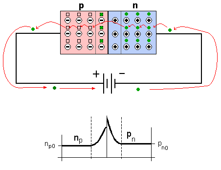
 direct polarization of the union P - N
 In this case, the battery will decrease the potential barrier space charge, allowing the passage of current of electrons across the junction, ie biased diode conducts electricity.
For a diode is forward biased, we must connect the positive terminal of the battery to the anode of the diode and the negative pole to the cathode. Under these conditions we observe that:
The negative terminal of the battery repels the free electrons of the crystal n, so that these electrons are directed towards the pn junction.
The positive terminal of the battery attracts the valence electrons of the crystal p, this is equivalent to saying that pushes the holes towards the pn junction.
When the potential difference between terminals of the battery is greater than the potential difference in space charge region, free electrons of the crystal n acquire enough energy to jump into the voids of the crystal p , which have previously been shifted to the pn junction.
Once a zone free electron n p skips to the area across the space charge, falls into one of the many gaps in the area becoming p valence electron. Once this occurs the electron is attracted to the positive terminal of the battery and move from atom to atom until the end p glass, from which enters the thread and reaches the battery.
Thus, with the battery giving free electrons ny area attract valence electrons in the p zone, appears across the diode with a constant current to the end. Bias: occurs when you connect the positive terminal of the battery to the union P of P - N and negatively to N.
 reverse polarization of the union P - N
 In this case, the negative terminal of the battery is connected to the area p and the plus to the area n, which increases the space charge region, and the tension in that area until it reaches the value of the battery voltage, as explained below:
The positive terminal of the battery attracts the free electrons in the region n, where n is out of the glass introduced into the conductor in which they move up to the battery. As free electrons leave the area n, the atoms that were previously neutral pentavalent, to be detached from its electron in driving orbital acquire stability (8 electrons in the valence shell, see semiconductor atom) and a net electrical charge of +1, which become positive ions.
The battery negative free electrons yields trivalent atoms in the area p. Recall that these atoms have 3 valence electrons, so that once the covalent bonds formed with the silicon atoms have only 7 valence electrons, being the so-called missing electron hole. The fact is that when the free electrons transferred from the battery enter the area p, fall into these holes with trivalent atoms gain stability (8 electrons in its valence orbital) and a net electrical charge of -1, thus becoming negative ions.
This process is repeated again and again until the space charge carries the same electrical potential as the battery.
In this situation, the diode should not conduct current, but due to the effect of temperature electron-hole pairs formed (see semiconductor) on both sides of the joint producing a small current (about than 1 uA) called reverse saturation current. In addition, there is also a stream called surface leakage which, as its name suggests, leads a small current through the diode surface, and that on the surface, the silicon atoms are not surrounded by enough atoms to make four covalent bonds necessary for stability. This causes the surface atoms of the diode, both in the area n and the p, with holes in its valence orbital so that the electrons flow easily through them. However, as is the reverse saturation current, surface leakage current is negligible.

CRF
Lenny Z. Perez M
0 comments:
Post a Comment